


Laboratory of Preparation and Characterization of Materials (LPCM)
- Home
- Research
- DFA - Department of Applied Physics
- Laboratory of Preparation and Characterization of Materials (LPCM)
Select your language

")
")


The Materials Preparation and Characterization Laboratory specializes in creating and analyzing semiconductor materials and nanostructures—the tiny building blocks that power modern electronics and photonics.
Our core work involves III-V semiconductors (materials made from elements in columns III and V of the periodic table, like gallium arsenide), which are essential for high-speed electronics and advanced light-based technologies.
We harness these special materials to create:
We also focus on integrating different materials into these nanostructures to unlock new and enhanced unctionalities.
We have deep, long-standing experience in cutting-edge fabrication techniques:
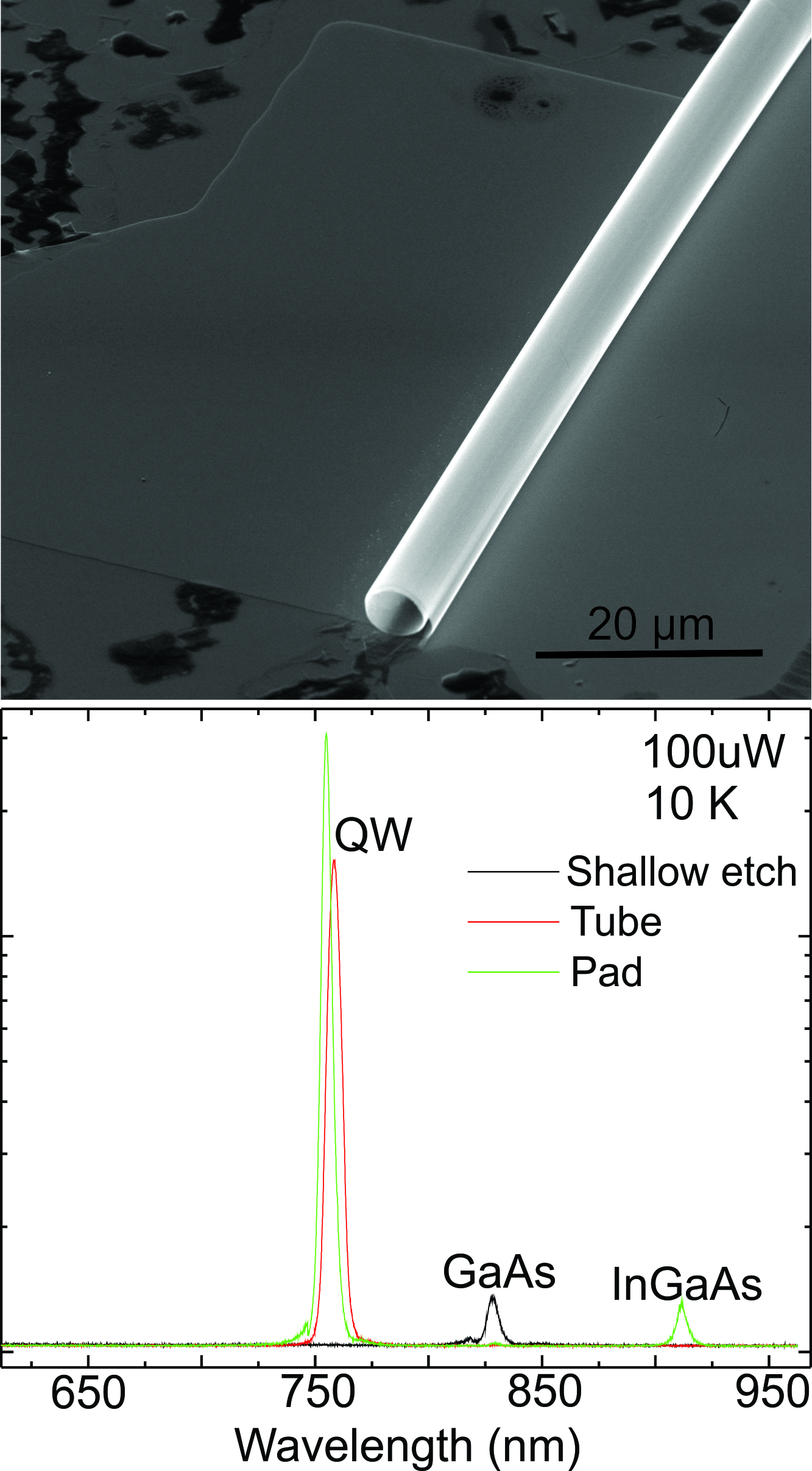
We are experts in rolling up our ultra-thin materials into nanotubes or microtubes. These tiny cylinders can act as highly efficient photonic structures—miniature light traps or resonators—that have potential applications in advanced sensors and communication.
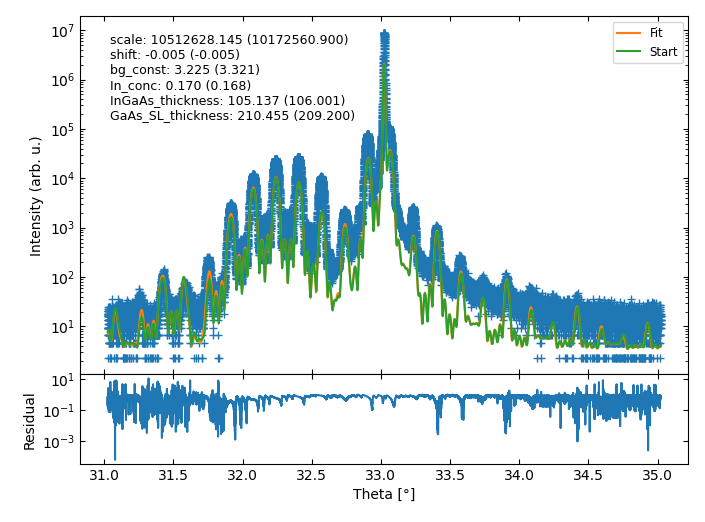
We use a sophisticated technique called Molecular Beam Epitaxy (MBE) to grow perfect, atomic-layer-by-atomic-layer III-V heterostructures (layered materials). This technique gives us ultimate control over the material's properties.
To ensure our materials are perfect, we use a suite of powerful characterization tools:
Universidade Estadual de Campinas - Instituto de Física Gleb Wataghin
Rua Sérgio Buarque de Holanda, 777
Cidade Universitária, Campinas - SP, 13083-859
Fone +55 19 3521-5297
Fax +55 19 3521-4147