


Laboratory of Photovoltaic Research (LPF)
- Home
- Research
- DFA - Department of Applied Physics
- Laboratory of Photovoltaic Research (LPF)
Select your language

")
")


Prof. Dr. Francisco das Chagas Marques (Group Leader)
Prof. Dr. Leandro Russovski Tessler
Prof. Dr. Luiz Fernando Zagonel
Photovoltaic Research Laboratory has basically three lines of research: photovoltaic conversion (devices that transform light energy into electrical energy, like solar panels), photonics (using light to transmit information, such as the devices used in optical communications) and research on new materials for the metalworking industry.
Photovoltaic conversion is the transformation of light energy into electricity. It happens to the solar cells (so-called solar panels are formed by several of them associated). In this "photovoltaic effect", the incidence of light on certain materials provides energy to electrons in the material and can be excited to the conduction band. Using a combination of two materials with different electronic levels, it is possible to obtain an electrical voltage between its ends, which generates an electric current when connected to a load.
The improvement of solar cells - the search for better efficiency, lower cost, smaller size, greater environmental security - involves the search for new photovoltaic materials, new coatings antirrefletores etc. The group acts in this type of research and studying optoelectronic, structural and thermomechanical properties of these new materials for application in solar cells and also in other electronic devices. This area requires the technology to manufacture thin films (lately, a few micrometers - thousandths of a millimeter - thick). The properties of the resulting system is crucially dependent on the method of formation of these films. Therefore, the techniques of deposition on a substrate thereof are also an important research in this front area, in which the group has improved their expertise.
The main materials studied are semiconductors - amorphous (non-crystalline) or nanostructured. Nanostructured materials are those having structures of up to a few nanometers in size, ie, up to some tens of atoms in diameter. Being so small, they present quantum effect not observed in the macroscopic scale and therefore may have very special properties. Exploiting these characteristics, its potential for application and what they can tell us about phenomena yet unknown about the basic physics is currently a large and active field of study.
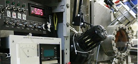
Deposition system designed and fabricated at IFGW for the deposition of diamond-like carbon (DLC) using the filtered cathodic vacuum arc (FCVA) technique
This is the search for hard material coatings such as carbon nitride, diamond-like carbon or silicon carbide. The idea is to get materials with mechanical properties and tribological getting better, which is increasingly required by the metalworking industry (which produces intermediate goods, metal, machinery, vehicles etc..). The emphasis is on development of materials and treat them to improve their performance.
A major group methods used by plasma nitriding is a process incorporating nitrogen atoms in the structure of the material near its surface. This decreases the friction between the parts of a mechanism and increases the hardness and corrosion resistance, fatigue and wear. Some of the main applications are in cutting tools, sintered parts, shafts, arrays, and prints.
The group also works with various alloys, made of carbon and different structures (diamond, polymer, tetrahedral), silicon, carbon, germanium nitride or carbon; also investigating materials such as doped (with low concentrations) boron, aluminum, phosphorus and nitrogen. The materials are developed in the laboratories of the group and are investigated for their characteristics, such as stress resistance, hardness, transmissivity of visible or infrared light and the profile shape of the material surface (profilometry).
The experimental methods used for these studies are the EXAFS (Extended Absorption Fine Structure of X-ray absorption spectroscopy type of X-ray, made at the National Synchrotron Light Laboratory, LNLS), RBS (Rutherford backscattering spectroscopy) Raman spectroscopy (the latter done in collaboration with other research labs), studies of luminescence and XPS (photoelectron spectroscopy, X-ray).
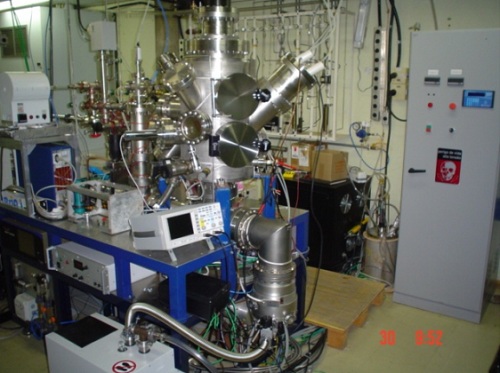
System ion beam deposition - Furthermore, the LPF Phenomena deposition and ion implantation materials, using relatively low energy ions (~ 10 eV to 1500 eV) by the technique of deposition assisted ion beam Dual (DIBAD, Dual Ion Beam Assiting Deposistion) using cannons Kaufman (see figure below).
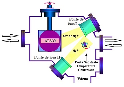
General scheme of the system DIBAD (dual ion beam).
The two ion sources are Kaufman type guns
General view of the real system
This machine has a rotating target holder to accommodate up to four different types of materials, allowing the multilayer film deposition by sputtering. The deposition process is assisted by two ion beams (produced by two cannons Kaufman type). A third type gun ECR (Electron Ciclotron Resonance) is on the back of the machine and is not visible in the drawing. The substrate is positioned by a precision xyz station and controlled temperature. The system is provided with handles for the transfer of samples. The DIBAD communicates with a system of ultra-high vacuum (UHV) for in situ analysis of the samples made by the technique fotoemitidos electron spectroscopy (XPS and UPS). The XPS system has lamp ultraviolet and X-ray study, respectively, the electronic structures of the valence band and core materials deposited by the technique DIBAD.
Carbon Nanotubes - The LPF also conducts research on carbon nanotubes deposited by the technique called Chemical Vapor Deposition Assisted Plasma (PECVD, Plasma Enhanced Chemical Vapor Deposition), for studies of electron emission induced by the electric field (field emission) . The nanotubes are analyzed by various techniques such as high resolution microscopy by transmission electron (HRTEM) and by scanning electron microscopy (SEM). Surveys are also directed to study the influence of the nanostructure of the substrate on the growth of nanotubes.
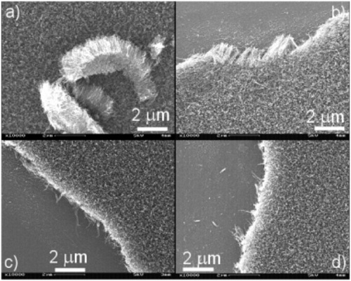
Carbon nanotubes. a) A "carpet" of nanotubes obtained after its extraction by a diamond and analyzed by SEM. b) A side view of the carpet. c) and d) by SEM Photos taken through a top view of the carpet.
Just as the word "electronic" refers to technologies based on the use of the electron energy and as a transmitter of information, the term "photonic" refers to technologies based on the use of light (photons) for the same purpose. The photonic device of the best known is the optical fiber. There is still much progress as possible in this area, although part of the communications now be made based on the transmission of light through these fibers, much of the information processing is still done with electricity - computers are still electronic, photonic and not.
Another challenge is that the demand for higher speed data transmission comes dangerously close the edge of current technology, which could mean the collapse of the Internet in a few years. There are projections that indicate if the network continue to move as it has in recent years, it is necessary to increase 100-1000 times the capacity of data transmission on the same. Otherwise, there may be a huge global congestion. To avoid this problem are being researched new materials for optical devices necessary for communication systems.
The new materials investigated by the group can serve two purposes - the optical communications and optical computing. The main used worldwide is silicon, since it is already the basis of microelectronics. However, if the electronic properties of semiconductor are very profitable, the optical properties are not good for photonics. However, when dopa silicon with tiny amounts of elements called rare earths, their optical properties are greatly improved. The group has investigated the Erbium as dopant. Devices based on silicon doped with erbium are already commonly used in research in photonics. Other dopants such as neodymium, are being explored, praseodymium, terbium and europium are also searched, along with other different arrays of silicon.
Lately, the team has also been dedicated to zinc oxide (ZnO) as a possible substitute of silicon. The advantage of ZnO is that it can form quite extensive and homogeneous nanowires. Nanowires are filaments having a thickness up to some tens of atoms. In this way, their optical properties are more interesting than with macroscopic sizes. Doping can also be used to improve their optical properties.
The group summarizes these systems and study their properties, how they change when changing the dopant, such as improving the synthesis method for better materials with improved optical characteristics, how to achieve a homogeneous doping concentration and controllable (sometimes not of the dopant evenly distributes the material and we need to find special techniques to enable it).
To perform these characterizations, the group uses equipment from the laboratory and the National Synchrotron Light Laboratory (LNLS). The main techniques are EXAFS the XANES (X-ray Absorption near edge Structure) - the latter two being two types of absorption spectroscopy, X-ray - and HRTM microscopy (High Resolution Transmission).
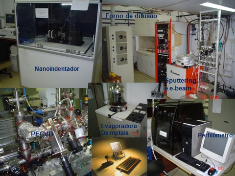
Equipment used in the LPF
Universidade Estadual de Campinas - Instituto de Física Gleb Wataghin
Rua Sérgio Buarque de Holanda, 777
Cidade Universitária, Campinas - SP, 13083-859
Fone +55 19 3521-5297
Fax +55 19 3521-4147