


Laboratory of Nano Biosystems (LNB)
- Home
- Research
- DFA - Department of Applied Physics
- Laboratory of Nano Biosystems (LNB)
Select your language

")
")


The Laboratory of Nano and Biosystems (LNB) focuses on the study of semiconductor nanomaterials, and research in biosystems. Linking these two issues, we have the intensive use of both electronic and scanning probe microscopies, and the fabrication of biosensors based on materials of interest to the group.
The synthesis of a particular type of material can be usually carried out with different techniques. In this group, growth is performed using epitaxial techniques, which is the gradual deposition of atoms or molecules on a substrate forming nanosize objects (nanowires, thin films, etc.). The research also includes the characterization which is the study of material properties obtained with these methods.
A widely used method for growth is the molecular beam epitaxy (CBE, or chemical beam epitaxy, in this case). In this method, molecules that contain atoms of the material to be formed reach a heated substrate where the material grows. For example, molecules containing arsenic and gallium can form a semiconductor microfilm comprising these two elements.
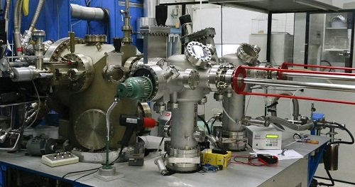
CBE Equipment, Applied Physics Dept., IFGW
The CBE technique can also provide information about the sample while it is formed. This technique - now in the field of characterization - is done with electron beams focused on the sample. Moreover, the research also includes a set of techniques to obtain very high resolution images commonly called scanning microscopes; they are able to distinguish structures with sizes of the same order as the diameter of an atom.
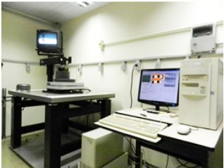
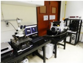
There are several types of scanning microscopes. The LNB has two equipments of Scanning Probe Microscopy, or SPM, which are shown in the pictures. In the most common type of measurement, called atomic force microscopy (AFM), a tip approaches the surface of the material, but does not touch it (there are other types of measurements where they touch each other). But the tip is so close to the surface that an attractive force appears between them, akin certain forces that hold molecules of substances together. The microscope system monitors the variation of this force as it scans the sample surface, canceling the variation by changing the vertical position of the sample. This vertical movement gives indications about the shape of the sample surface, creating a map thereof. Depending on how the measurement is made (and which tip is used), one can obtain maps of different sample features that enable the characterization of their electrical properties, magnetic and mechanical properties, for example, at the nanometer level.
Equipamento de Microscopia de Varredura por Sonda para análise de amostras em ar.
Detalhe da alavanca que segura a ponta (abaixo dela) onde o laser que monitora a medida pode ser observado.
Equipamento de Microscopia de Varredura por Sonda para análise de amostras em atmosfera controlada ou em solução
Besides these facilities, the group supports and often uses the Multi-User Lab (LAMULT) of IFGW, with access to a wide range of characterization techniques and processing. Another facility widely used in the LNB research projects is the Electron Microscopy Laboratory of the LNNano/CNPEM. Through this multi-user facility, the LNB personnel has access to both type of microscopes, scanning (which show the sample surface) and transmission electron microscopes, which allows the evaluation of the sample structural properties (crystallinity, for example) with atomic resolution.
With current technology, we can produce new materials with unique properties suitable for various purposes. The academic research in this area improve methods to synthesize these materials and study their characteristics. In many laboratories in the world, it is possible, under certain conditions, to design materials that do not yet exist in order to provide properties of interest for specific application (research on "functional materials"). Often, the procedure is to use certain regularities already known as a base to guide research.
Among the interesting phenomena in this field, two which are well exploited in these studies are the interfaces, ie the junctions between different materials, and the size effects. The latter are important for materials with structures (or "details") very small, on the order of tens or hundreds of atoms across - such as nanowires, nanotubes and quantum dots. The word "nano" here refers to the size of billionths of a meter.
When a material form such small objects, their properties may significantly differ from the "large" objects (or as they are called in literature, the "bulk"). The reason is that in nanometric objects, their surface characteristics show important effects on the material properties as a whole. The surface of the objects may have very different properties from the bulk - see, for example, the surface tension of water. The nanostructures therefore constitute new possibilities for materials with new features still to be studied and explored.
Among the nanostructures investigated in the group are semiconductor nanowires (figure below). The nanowires are made of one or more semiconductor materials, up to several microns in length and several tens of nanometers in width. Nanowires, as well as a more conventional semiconductor structure in the form of a multilayer of thin films, can have quantum dots in their structure. These dots can have many shapes; in one of them small semiconductor particles (or nanocrystals) are inserted within another semiconductor material. The quantum dots act as "traps" inserted inside a semiconductor material, and are capable of trapping electrons (which otherwise would be free to, for example, conduct electricity).
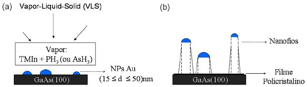
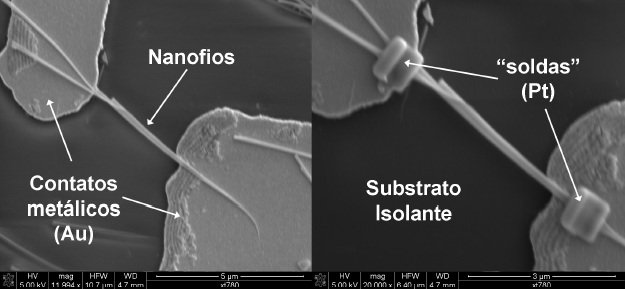
Semiconductor nanowires. Above: Schematics of how the nanowires are grown. Small gold particles (called catalysts) are placed on the substrate, with diameters typically between 5 and 100nm. The atoms of indium and arsenic molecules which reach the substrate (in the technique CBE) incorporate preferentially into the gold particles making the wire grow faster than the film on the substrate around. Below: a nanowire of indium and arsenic metal contacts is mounted on gold (Au) pads, with "welds" made of platinum (Pt) holding it in place on the insulating substrate. The assembly of this device was performed using the equipments of the Center for Semiconductor Components at Unicamp by Murilo Neves de Martins.
Source: M.Sc. Dissertation from Angela Narváez Carolina González, IFGW/Unicamp (2008), pages 17 and 54.
The LNB group also investigates biomaterials and biological systems. It is possible to use for this research the same equipments used for the study of semiconductor materials. The idea is to use complementary techniques to those already used by biologists and materials engineers in order to add information to existing studies, in an original approach. One example is the study of the growth of the bacterium Xylella fastidiosa - or Xf – on a cellulose surface, instead of glass, as is usually done in biology laboratories. This research can improve the understanding on how the cell gets fixed on a substrate (Xylella causes the citrus variegated chlorosis (CVC), also known as ‘amarelinho’, in citrus fruits). This study is carried out in a collaboration with the Citrus Center from the Agronomic Institute of Campinas. One of the advantages is that the pool of techniques used in the LNB group - including fluorescence microscopy - allows the observation of living cells, as shown in the (A) image.
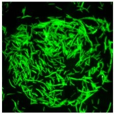
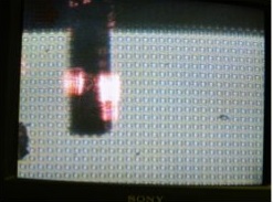
(A) Imagem de microscopia de fluorescência mostrando estágios iniciais de biofilmes de bactérias Xf vivas que expressam GFP, proteína que fluoresce no verde (magnificação=60X)
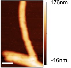
Imagem AFM de células de Xf aderidas em vidro
In addition, the LNB today has a large infrastructure (exhaustion hood, laminar flow, incubator, autoclave, etc.) for the preparation of samples in the laboratory, as illustrated by the following images.
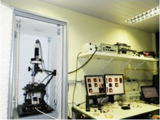
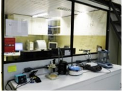
Fotos do laboratório mostrando o microscópio de fluorescência e estação de pontas para medidas em dispositivos
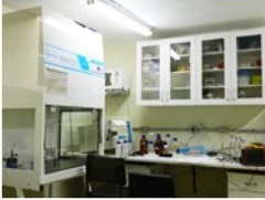
Infra-estrutura de apoio à preparação de amostras biológicas
Infra-estrutura de apoio à preparação de amostras biológicas
Another example on this line of research is the investigation on the interaction of chemical compounds with cell membranes. For this, artificial membranes are made similarly to those of living cells (they are called model membranes), but deposited on a solid surface. One can then investigate, in real time, changes on their properties when in contact with different amounts of new substances: changes in the chemical composition of the membranes, in their shape and elasticity. Below, images of the action of a local anesthetic, dibucaine, in a model membrane. There is also research on other subjects, especially nanobiodevices, which may provide several applications and are still being explored. Nanotechnology and nanoscience are two very promising areas for applications ranging from pharmacology to electronics. The LNB group also focuses on the study of nanosensors because they can provide much greater sensitivity than conventional devices, precisely due to the important role that the surface (which makes the sensing) has in the device properties as a whole. The research encompasses nanosensors which can diagnose, for example, if one had a subtle case of heart attack in the first paramedical care, by means of measuring and analyzing the concentration of several enzymes or proteins in this person’s blood. Nanosensors can also be used for environmental monitoring (detection levels of pollution and contamination, including pathogens in plants).
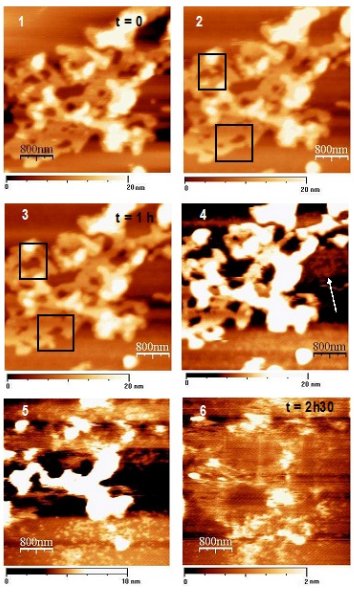
Model membrane (multiple lipid bilayers supported by mica substrate) observed by atomic force microscopy in aqueous solution. At t = 0, local anesthetic (dibucaine) was added in small concentration into the liquid cell where the membrane was placed. Subsequent images show incomplete bilayers (with lighter color) that gradually disappear with time due to the action of anesthetic (arrows). After about 3hs the incomplete bilayers disappear completely and the bottom layer already shows signs of change in structure by the action of the anesthetic molecule.
Source: Dissertation Gabriela Simone Lorite, IFGW / Unicamp (2007), p. 45
Universidade Estadual de Campinas - Instituto de Física Gleb Wataghin
Rua Sérgio Buarque de Holanda, 777
Cidade Universitária, Campinas - SP, 13083-859
Fone +55 19 3521-5297
Fax +55 19 3521-4147